FPGA vs CPU for real time power electronics simulation
Power Electronics
03 / 09 / 2026
Key Takeaways
- Start the CPU versus FPGA choice with fixed time step, worst-case latency, and jitter limits, since missed deadlines will invalidate HIL results faster than any modelling compromise.
- Use CPUs for fast iteration, larger multi-domain models, and frequent updates, and use FPGAs when switching, protection, and I/O timing must stay deterministic on every sample.
- Get the best cost and schedule outcomes with disciplined partitioning, keeping only timing-critical paths on FPGA while leaving the rest on CPU so your team can debug and update models without friction.
Pick a CPU when your model needs flexibility, and pick an FPGA when it needs deterministic sub-microsecond timing.
That choice matters because real time power electronics simulation is rarely limited by math alone; it’s limited by time step, I/O timing, and how much switching detail you keep. Power electronics already process about 70% of the electricity used in the United States, which is why validation pressure lands on power stages, controls, protection, and grid interaction at once. If your simulator misses deadlines, your controller test becomes a timing test, not a controls test.
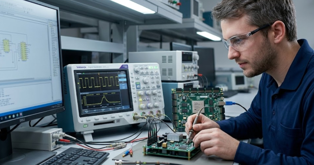
CPU-based simulation will cover a lot of hardware-in-the-loop (HIL) work because it’s fast to build, iterate, and debug. FPGA-based simulation earns its keep when your switching, sensing, or protection paths must behave like hardware on every sample, with tight bounds on latency and jitter. Teams that treat this as a partitioning and timing problem, not a processor rivalry, get to stable results faster.
Match solver time step targets to CPU or FPGA
A CPU fits best when your fixed time step can sit in the tens of microseconds and still meet your test goals. An FPGA fits best when your fixed time step must drop into single-digit microseconds or below and still hit every deadline. The first decision is not fidelity, it’s scheduling. If the simulator can’t complete each step on time, the results stop being trustworthy.
Start with the fastest loop that must be closed in real time, then work outward. Gate-drive and protection logic pushes you to the smallest time steps, while thermal or energy management models tolerate larger steps. CPU solvers handle many continuous states well, and they shine when you need to swap model variants daily, tune parameters live, or run batch sweeps across cores. FPGA solvers shine when parallel, fixed-latency execution matters more than floating-point convenience.
Time step selection also shapes what you can represent without numerical artefacts. Switching edges that are “too sharp” for your step will smear into the next sample and distort current ripple and peak values. If your goal is controller stability and average power flow, a larger step and an averaged model can be the right call. If your goal is protection timing or current limiting on a cycle-by-cycle basis, the time step sets a hard floor on what a CPU can deliver.
Compare latency, jitter, and I/O timing requirements
“The main difference between CPU and FPGA timing is determinism.”
A CPU can deliver low average latency, but it will show jitter from scheduling, interrupts, and bus contention unless the full stack is engineered for determinism. An FPGA executes logic with predictable timing that you can bound in advance. If your test cares about worst-case timing, jitter matters more than average speed.
I/O timing often becomes the hidden requirement. Analog and digital I/O sampling must line up with the solver step, and actuator updates must land at consistent instants if you’re validating fast protection or PWM synchrony. CPU systems can keep tight timing when the model is light and the software stack is tuned, but heavy models and background activity increase jitter risk. FPGA I/O can be clock-aligned, which keeps sampling, latching, and edge detection consistent across runs.
| If this is true in your test | The safer compute choice is usually |
| Your fixed time step can be 25–100 microseconds without hiding faults. | A CPU, because you’ll iterate faster and keep modelling options open. |
| Your protection logic must react within a few microseconds every time. | An FPGA, because bounded latency beats “fast on average” timing. |
| Your I/O must line up tightly with PWM edges and sampling instants. | An FPGA, because clocked I/O reduces jitter and phase drift. |
| Your validation depends on large networks, filters, or multi-domain models. | A CPU, because memory and floating-point throughput scale cleanly. |
| You need mixed fidelity, with some parts fast and others detailed. | A split CPU plus FPGA, because each side can carry what it suits. |
| You expect frequent model edits and frequent test procedure updates. | A CPU first, then move only the timing-critical parts to FPGA. |
Assess model fidelity limits for switching power converters
Model fidelity is a budget you spend in computation and timing margin. CPU simulation handles averaged and phasor-style models well, and it can handle switching models only if the time step stays manageable. FPGA simulation is built for switch-level logic at very small time steps, but you trade away some modelling convenience. The right target is the simplest model that still answers your test question.
Switching devices keep getting faster, and that pushes timing pressure into the simulator. Switch transitions near 50 ns have been demonstrated in silicon carbide devices, which shows how much detail can exist inside a single microsecond of behaviour. You won’t simulate nanosecond edges in real time, but that speed highlights why dead time, diode recovery, and dv/dt-related effects can be sensitive to solver step choices. If your acceptance criteria include peak current, overvoltage trips, or blanking times, you’ll feel those limits quickly.
Fidelity decisions also change what you can validate with confidence. Averaged models will give clean control-loop tuning and power flow behaviour, yet they can hide cycle-level faults and switching ripple that interacts with current sensing. Switching models capture those effects, but they can force you to simplify elsewhere to keep deadlines. A practical approach is to align fidelity with the signal you’re judging, then treat any extra detail as a risk to real-time execution unless you can prove it stays stable across operating points.
“Pick a CPU when your model needs flexibility, and pick an FPGA when it needs deterministic sub-microsecond timing.”
Plan partitioning between CPU and FPGA in HIL setups
Partitioning works when you put each task on the processor that matches its timing needs. Fast switching and protection paths belong where execution is deterministic, while slower plant dynamics and supervisory logic belong where modelling is flexible. The interface between them must be sampled, scaled, and synchronized with intent. If the boundary is sloppy, you’ll chase artefacts that look like control issues.
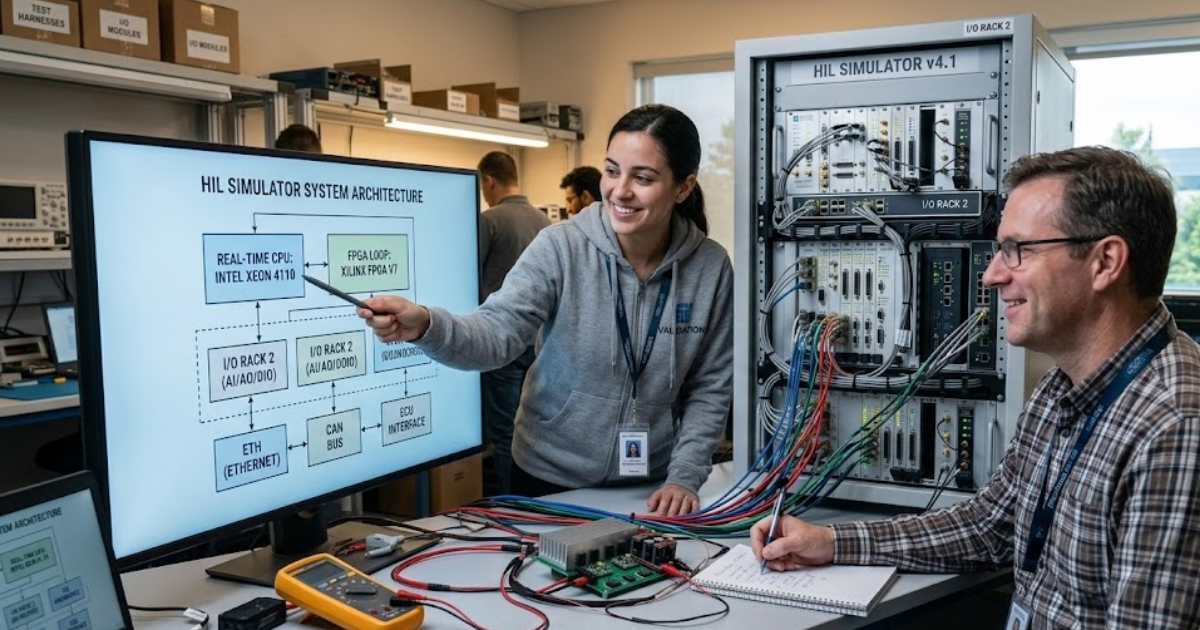
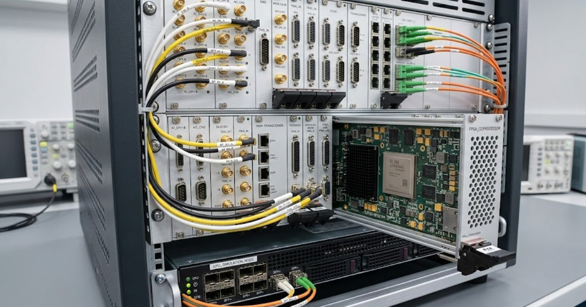
A concrete pattern shows how this plays out. A team validating a 2-level grid-tied inverter can run the PWM generation, comparator-style overcurrent protection, and switch-level power stage on FPGA at a sub-microsecond step, while the grid impedance, phase-locked loop, and power calculations run on CPU at a larger step with rate transitions. That split keeps tight timing where protection and switching need it, while preserving CPU headroom for test automation and parameter sweeps. OPAL-RT systems are often used in this mixed compute style because they support CPU and FPGA execution under one HIL workflow, which makes that boundary easier to engineer without inventing custom plumbing.
Plan the boundary like an I/O contract, not a software convenience. Decide what signals cross the CPU to FPGA line, pick explicit sample rates, and define how you handle quantization and saturation. Latency must be counted end-to-end, including A/D, solver step alignment, and D/A updates. When you treat partitioning as timing architecture, you’ll know which part of the system is responsible for each microsecond of delay.
Account for toolchain, debugging, and model update effort
CPU models update quickly, and the debugging loop looks familiar to most engineering teams. FPGA models take more upfront planning because compilation, resource limits, and fixed-point choices become part of the engineering work. That effort pays off when you need deterministic timing, but it will slow iteration if you move too much too early. A staged approach keeps the project moving while you lock down what must be deterministic.
Debugging also feels different. CPU workflows support breakpoints, profilers, and fast rebuilds, while FPGA workflows rely more on assertions, signal capture, and careful verification of timing and scaling. Model changes that are trivial on CPU can require retesting numeric ranges, checking saturation behaviour, and validating I/O alignment on FPGA. Teams get smoother results when they treat FPGA work like embedded design with formal checks, not like a last-minute performance patch.
- Your smallest required time step and the worst-case compute margin at that step.
- Your worst-case allowed jitter on PWM, trips, and sampled protection signals.
- Your plan for fixed-point range, scaling, and saturation checks.
- Your expected frequency of model edits after the first stable baseline.
- Your ability to reproduce timing and numeric behaviour across test benches.
Cost and schedule risk usually come from workflow friction, not from raw compute. CPU work can sprawl if you keep adding detail until deadlines slip, while FPGA work can stall if you start with too much scope and too little verification structure. Put guardrails around what “done” means for timing, fidelity, and I/O behaviour. That discipline keeps the team aligned when test results get noisy.
Choose a HIL simulation platform that scales with projects
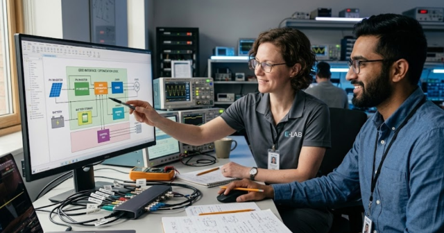
A HIL platform will serve you well when it lets you hit timing deadlines, maintain traceable model behaviour, and keep iteration speed high as projects grow. CPU capacity alone won’t save a test bench that needs deterministic I/O, and FPGA determinism alone won’t save a bench that needs constant model changes and multi-domain scope. The best choice is usually a platform that supports CPU and FPGA compute and lets you move boundaries without rewriting everything. You’re buying a repeatable execution model more than a processor type.
Focus on a few platform traits that affect daily work. Deterministic I/O timing, clear rate-transition handling, and reliable synchronization tools will matter every week. Hardware modularity matters because channel counts and sensor types tend to expand across programs. Software openness matters because your team will connect MATLAB, Python, test sequencers, and data pipelines, and closed stacks turn simple integration into a project.
Good engineering judgement shows up in how you keep the simulator honest over time. Lock down timing budgets early, then add fidelity only when it changes a pass or fail outcome. Keep CPU models flexible for learning and keep FPGA models focused on the parts where determinism is non-negotiable. OPAL-RT fits this execution-first mindset when you need both compute types available on the same bench, so you can treat FPGA as a precise timing tool and CPU as an iteration tool, instead of forcing one to do both jobs.
Real-time solutions across every sector
Explore how OPAL-RT is transforming the world’s most advanced sectors.

Simulation
03 / 30 / 2026
Understanding timestep requirements for modern power converters
Practical criteria for selecting EMT and real time simulation timesteps for power converters, covering switching resolution, control and PWM timing alignment, multirate approaches, and verification checks.
Industry applications, Simulation, Energy
03 / 29 / 2026
Validating data center energy management systems using real-time HIL
This piece explains how AI workload variability affects data centre power stability and how closed-loop HIL testing helps validate EMS control behaviour under site and grid stress.
Industry applications
03 / 28 / 2026
Control algorithm validation using real-time HIL
A practical look at how real-time HIL testing validates embedded control algorithms through closed-loop simulation, fault reproduction, digital plant models, and disciplined integration.
EXata CPS has been specifically designed for real-time performance to allow studies of cyberattacks on power systems through the Communication Network layer of any size and connecting to any number of equipment for HIL and PHIL simulations. This is a discrete event simulation toolkit that considers all the inherent physics-based properties that will affect how the network (either wired or wireless) behaves.