
Key Takeaways
- Wide bandgap devices raise power density through a chain that runs from lower switching loss to higher frequency to smaller passives, and each link sets its own limit.
- Heat flux and parasitic inductance become the binding constraints once magnetics shrink, so efficiency and packaging have to be designed as one problem.
- Dense SiC and GaN converters need validation that resolves individual switching edges, because slower test models hide the timing faults that density exposes.
Wide bandgap devices raise converter power density because they cut switching loss far enough to let you run faster, and faster switching shrinks almost everything around the transistor.
The gains are large enough to reset expectations. A research team recently packed 500 kW into a 1 L inverter built on silicon carbide (SiC) switches, a result its designers put at 2.5 times the best systems available. Numbers like that come from a chain of decisions that starts at the device and runs through the magnetics, the capacitors and the cooling path.
Each link in that chain gets tighter as the box gets smaller, and the tightest link is usually proof. A dense design in power electronics leaves you less margin for layout error, thermal error and control timing error. Your test bench has to resolve events that last tens of nanoseconds, or the density you gained on paper won’t survive the first prototype. Density is earned at the device and kept at the bench.
What wide bandgap semiconductors are in practical terms
Wide bandgap semiconductors are materials such as SiC and gallium nitride (GaN) that need roughly 3 times more energy than silicon to free an electron. That property lets a device block the same voltage with a much thinner active layer, so it conducts with less resistance and stores less charge.
Picture two 650 V switches with the same on-resistance, one silicon and one GaN. The GaN part uses a far smaller die, which means less capacitance to charge and discharge on every transition. Less charge moved per cycle is less energy lost per cycle, and that saving repeats hundreds of thousands of times each second.
SiC and GaN split the voltage range between them. SiC handles the 800 V to 1,700 V classes found in traction inverters and grid converters, and it tolerates heat well. GaN fits best at 650 V and below, where its speed matters most. You’ll pick between them on voltage first and frequency second.
Why a GaN FET switches faster than silicon
A GaN FET switches faster than silicon because it has very little gate charge, very little output charge and no reverse recovery charge to clear. Current flows through a thin sheet of highly mobile electrons at the surface of the device, so the channel opens and closes in a few nanoseconds.
Measured results back this up. Engineers at a national laboratory built converters around GaN parts that switch 10 to 20 times faster than silicon while losing less energy, with data centre power conversion as the stated target. Reverse recovery is the detail that matters most in hard-switched bridges such as a totem pole stage. A silicon MOSFET body diode dumps stored charge into the opposite switch at every commutation, and that loss grows in step with frequency. GaN doesn’t have that penalty, so the frequency ceiling moves up.
How higher switching frequency shrinks the magnetics inside a converter
Higher switching frequency shrinks magnetics because an inductor or transformer only has to hold energy for one switching period. Shorten the period and the component needs less inductance, fewer turns and a smaller core to deliver the same power at the same ripple.
Take a generic 48 V to 12 V buck stage with 4 A of ripple current as an illustration. At 100 kHz, the inductor works out to about 22.5 µH. At 1 MHz the same ripple needs 2.25 µH, a 10 times reduction in inductance.
Volume doesn’t fall by the same factor. Core loss per unit volume climbs with frequency, and winding loss rises as current crowds toward the conductor surface. You’ll often move to a different ferrite, litz wire or a planar winding built into the circuit board just to hold temperature.
Capacitors follow the same logic with their own floor. Filter capacitance drops with frequency, yet the DC link still has to carry ripple current and survive its hot spot temperature. The honest gain is a smaller passive set that runs closer to its limits.
What limits converter power density once the passives shrink
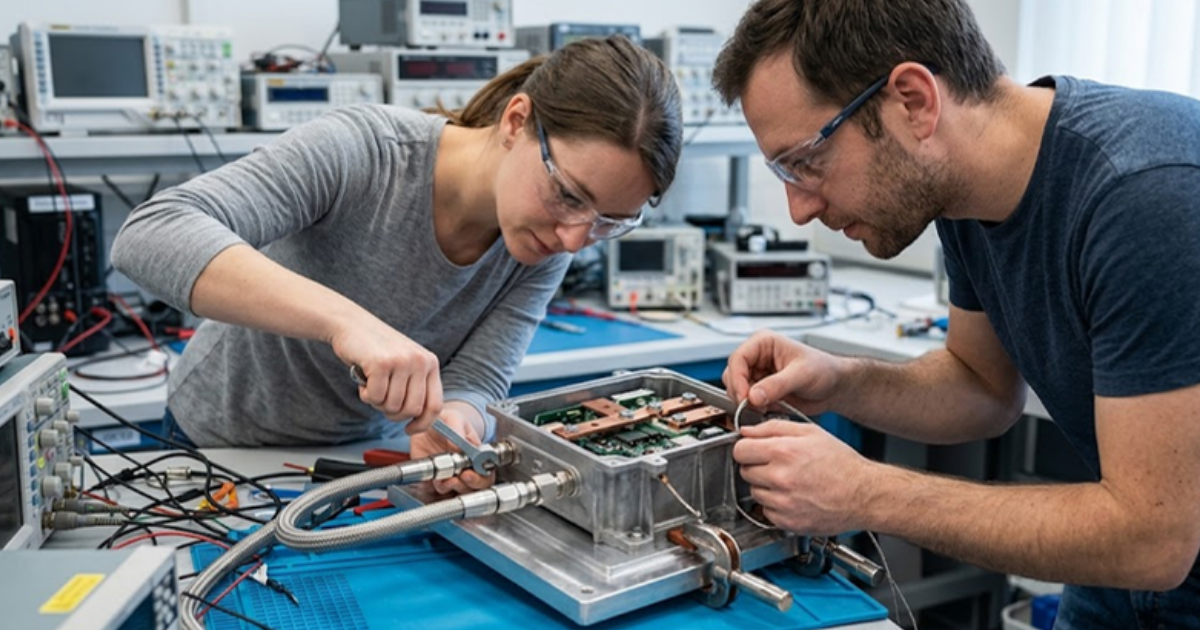
Heat removal and parasitic inductance limit converter power density once the passives shrink. Loss that used to spread across a large heatsink now leaves through a few square centimetres of die and board, and every nanohenry in the switching loop turns fast current edges into voltage overshoot.
A 10 kW converter at 99% efficiency still sheds about 100 W. At 98% that figure doubles, and so does the cooling hardware.
“Efficiency and density are the same problem seen from two sides, which is why a 1% loss is worth a redesign.”
| Link in the density chain | What tightens as the converter shrinks |
| Switching device | Smaller dies concentrate loss, so junction temperature rises faster after a load step. |
| Inductors and transformers | Core and winding loss set the size floor long before the inductance value does. |
| Capacitors | Ripple current rating and hot spot temperature decide how small the DC link gets. |
| Layout | Loop inductance converts fast edges into overshoot that eats your voltage margin. |
| Cooling path | Heat flux per square centimetre climbs even when total loss falls. |
| Control timing | Dead time and sampling delay take a larger share of each switching period. |
Layout shows the limit in numbers. A 10 nH loop carrying current that slews at 2 A per nanosecond produces 20 V of overshoot, and a faster device makes that worse. The remedy is tighter packaging, which pushes parts closer and raises the thermal stakes again.
Where power density pays off first in electrified products
Power density pays off first where volume or weight carries a direct cost, which means vehicles and server power supplies. An onboard charger that shrinks leaves room for battery cells, and a denser supply delivers more watts to a rack without taking more shelf space.
The two cases pull on different devices. An 800 V traction inverter leans on SiC because the bus voltage and the heat under the hood rule out most alternatives. A server supply uses GaN in its front end and its isolated DC/DC stage, where frequencies of several hundred kilohertz make the transformer small enough to fit a 1U profile. Both programs share one constraint. The design that wins is the one that reaches its efficiency target at the size the product allows, and that target leaves very little room for a late respin.
What gets harder to validate at high switching frequency
Timing resolution gets harder to validate at high switching frequency, because the events that decide loss and stability shrink faster than the test equipment’s ability to see them.
“A simulator that steps slower than the switching period averages away the behaviour you need to check.”
Consider a 500 kHz stage with a 2 µs period. A hardware-in-the-loop model that updates every 10 µs can’t place a single gate edge, let alone a 50 ns dead time that already equals 2.5% of the period. Your controller sees a smoothed plant and passes tests it would fail on real hardware.
Five checks become harder as frequency climbs.
- Gate edge placement relative to the simulation timestep
- Dead time effects on current distortion
- Protection response to a cross-conduction fault
- Control loop delay from sampling to pulse-width modulation update
- Resonant tank behaviour near the edge of soft switching
FPGA-based solving closes that gap. OPAL-RT built the eHS solver to track high-frequency switching on FPGA in real time, so your SiC and GaN controller is exercised at the speed the converter runs. That fidelity matters most for the faults you can’t safely stage on a prototype.
Validation speed decides how far a dense design goes
Validation speed decides how far a dense design goes because every gain in density removes margin that used to hide mistakes. The device lets you switch faster, and the bench has to keep up, or the unverified corners of the design become field failures.
The same pattern shows up across converter programs of every size, and it’s easy to spot. Teams that treat the device as the whole story spend their schedule on board respins. Teams that plan the chain from die to passives to cooling to test catch the hard problems while they’re still cheap to fix. A controller proven against a plant model that resolves each switching edge arrives at power testing with far fewer surprises.
That’s the discipline wide bandgap asks of you. Choose the device for the voltage and frequency you need, size the magnetics for loss as well as inductance, and give heat a short path out. Then test at the speed the hardware runs. OPAL-RT supports that last step with real-time simulation fast enough for the converters you’re building now.
Power Electronics
10 / 15 / 2026
Flying capacitor converter simulation for multilevel designs
How a flying capacitor converter balances its capacitor voltages through switching, where that balance breaks, and what a switching-accurate simulation has to capture.

Industry applications
10 / 12 / 2026
Validating eVTOL electric propulsion before the first flight article
A walk through motor, inverter and battery validation for eVTOL aircraft and the points where real-time simulation carries propulsion evidence ahead of flight test.
Power Electronics
10 / 11 / 2026
Totem pole PFC design and real time validation
How a totem pole PFC works, why its control is hardest at the AC zero crossing, and how real-time testing checks that transition before hardware is built.