Capturing GaN switching transients in real time converter models
Power Electronics
09 / 12 / 2026

Key Takeaways
- Switching loss, voltage margin and conducted emissions are all integrals across the commutation edge, so timestep selection decides how far those numbers can be trusted.
- Averaged models under report loss in one direction, which makes optimistic thermal results a systematic risk rather than a random error.
- Fine resolution belongs on the converter stage while the surrounding grid or machine model runs coarser, keeping finite FPGA resources aimed at the fastest physics.
A GaN converter model earns its value only when the switching edge stays sharp enough to read.
Most three phase grid connected power electronics still switch below 20 kHz, while the United States Department of Energy now points wide bandgap hardware toward more than 500 kHz by 2035 at power levels above 500 kW. Every step up in switching speed shortens the window a simulator must resolve, and GaN devices commutate in a few nanoseconds. A model that steps in microseconds averages that edge away and hands you a clean waveform hiding the losses, ringing and noise you wanted to measure.
Edge fidelity is a modelling choice you make before the first run, and it sets how much of your hardware behaviour you’ll ever see. Designers who treat the switching interval as the unit of accuracy get efficiency numbers and EMI predictions they can act on. Those who treat it as rounding error pay the difference later on the bench.
What a GaN switching transient contains and how fast it moves
A GaN switching transient is the few nanoseconds in which the device moves between full block and full conduction, carrying steep dv/dt and di/dt, gate ringing and package inductance effects. Most of a converter’s switching loss and conducted noise energy sits inside that short window.
A 650 V enhancement mode GaN transistor in a 1 kW totem pole power factor correction stage slews several hundred volts in under five nanoseconds, and loop ringing settles over the next twenty to forty nanoseconds. Read that interval at 10 ns and you’ll see a step. Read it at 250 ps and you’ll see the peak, the ring frequency and the loss integral.
The numbers engineers argue over are all integrals across that edge. Switching loss is the product of voltage and current through the commutation interval, peak voltage sets margin against the device rating, and ring frequency sets the first emissions peak. Lose the shape of the edge and all three become estimates.
Why coarse simulation timesteps erase the detail designers need
A simulation timestep acts as a low pass filter on everything it samples. When the step is longer than the transient, the solver reports an averaged value across the interval, so the peak disappears, the ring is never sampled and the loss integral collapses toward the ideal case.
A 10 µs step in a 100 kHz GaN converter gives you ten samples per switching period, which describes the fundamental and not the edge. Useful edge shape starts appearing near 10 ns to 25 ns, roughly two hundred times finer than the switching period. Averaged models don’t scatter around the truth, they sit below it, because every neglected peak and unsampled ring cycle removes energy from the result. Teams that size heatsinks from that output run warm on the bench and can’t tell if the error came from the device model, the thermal network or the timestep.
“Averaged models don’t scatter around the truth, they sit below it, because every neglected peak and unsampled ring cycle removes energy from the result.”
How solver architecture sets the limit on transient fidelity
The timestep floor is set by how much of the converter model the solver computes between steps. CPU based real time solvers settle around 10 µs to 50 µs. FPGA based solvers run the switching stage in parallel logic and reach nanosecond steps, which is the range a GaN edge requires.
The split matters most in hardware in the loop work. A three phase inverter model on a general purpose processor spends its step budget solving the network in sequence. Move the switching stage onto FPGA fabric and the same converter resolves at 250 ns or below, so the controller sees edges shaped the way hardware shapes them. OPAL-RT built the eHS solver around that split, computing the power stage in FPGA logic while the slower plant model stays on the processor.
The tradeoff is model size. FPGA resources are finite, so a nanosecond class solver holds a bounded number of switches and nodes. You’ll get the edge fidelity, and you’ll plan the partition around it, usually putting only the converter stage under fine resolution.
Choosing between averaged and switching level converter models
The main difference between an averaged model and a switching level model is what each one discards. An averaged model replaces the switching action with its mean effect over a period, which runs fast and stays stable. A switching level model computes each commutation, which costs computation and returns loss, ringing and noise content.
Both belong in a program, at different points. Control loop bandwidth studies run happily on averaged models at 50 µs, because the loop dynamics you’re checking sit well below the switching frequency. Thermal sizing, EMI pre compliance and gate drive validation need the edge.
| What you are testing | Model resolution that fits | What the choice costs you |
| Control loop stability across a wide operating range | Averaged model at 20 µs to 50 µs steps | Switching loss and conducted noise are absent |
| Junction temperature and heatsink sizing | Switching level model near 250 ns or finer | Model size stays bounded by FPGA resources |
| Conducted EMI pre compliance screening | Switching level model with package parasitics | Setup time rises and each layout revision needs new extraction |
| Gate drive timing and dead time tuning | Switching level model at nanosecond resolution | Only the converter stage fits, so the plant runs coarser |
| Grid code studies across many minutes of operation | Averaged model with an equivalent loss term | Individual edge behaviour cannot be inspected at all |
The cost of getting this wrong runs in one direction. An averaged model used for thermal work under reports loss and produces optimistic junction temperatures, and that hardware reaches the lab running hot.
How edge resolution shapes efficiency and EMI predictions

Efficiency and EMI results are decided inside the switching edge, so they inherit the resolution of the model that produced them. Switching loss scales with the overlap of voltage and current during commutation, and conducted emissions peaks follow the ring frequency set by loop inductance and device capacitance.
The efficiency gap GaN opens is small in percentage terms and large in consequence. A GaN laptop charger measured under the International Energy Agency 4E programme reached 86% against 81.4% for its silicon equivalent, and that margin comes almost entirely from shorter commutation intervals. A model that smooths those intervals reports both devices as nearly identical, which removes the reason for picking GaN at all.
EMI carries the same exposure. The first conducted emissions peak for a fast GaN edge often sits between 30 MHz and 100 MHz, which a 1 µs model cannot represent because its sampling ceiling is 500 kHz. Teams that find this after the pre compliance scan rebuild the filter late.
“Efficiency and EMI results are decided inside the switching edge, so they inherit the resolution of the model that produced them.”
Common mistakes that hide switching losses in converter simulation
Most missed switching loss traces back to modelling shortcuts rather than a wrong device datasheet. Ideal switch elements, absent parasitic inductance, fixed junction temperature and timesteps picked for solver stability instead of physics all push reported loss below what the hardware produces.
These five show up most often in converter work.
- Ideal switch elements with zero transition time, which report switching loss as zero regardless of device speed.
- Commutation loop inductance left out, which removes the voltage peak and the ring that set margin and noise content.
- A timestep picked to keep the solver stable rather than to sample the transition, so the edge is averaged before measurement.
- Junction temperature held constant through the run, which understates conduction loss as the device heats under load.
- Reverse conduction in GaN handled with a silicon body diode model, which misses the higher third quadrant drop during dead time.
Each one is individually defensible and collectively expensive. A model carrying all five reports a 1 kW GaN stage at 99% efficiency when the bench measures 97.5%, and the 15 W difference lands on a heatsink never sized for it.
What disciplined transient capture gives an engineering team
Teams that resolve the switching edge early stop rediscovering the same problems on the bench. Thermal margin, filter sizing and gate timing get settled while they are still cheap to move, and the hardware build starts from numbers that already survived scrutiny.
The value compounds across a program. A converter model reporting honest loss at 250 ns resolution becomes the reference every later decision leans on. When the prototype measures within a watt or two of it, you stop arguing about the model and start arguing about the design. That’s a quieter benefit than a faster simulation, and it’s the one experienced teams protect.
Real time platforms from OPAL-RT sit in that workflow because the FPGA solver keeps the edge visible while a physical controller stays in the loop, so what you validate in simulation is what the controller meets in hardware. The discipline matters more than the platform though. Pick the resolution the physics requires, keep coarse models for the questions that deserve them, and the switching transient stops being the part you find out about last.

Power Electronics
09 / 30 / 2026
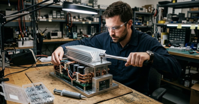
FPGA simulation for power electronics and motor drives
A technical comparison of CPU and FPGA solver architectures for power electronics and motor drive simulation, covering the timestep each reaches and how to split a model between them.
Power Electronics
09 / 29 / 2026
How to model and control a T-type three level inverter
An engineering overview of the T-type three level inverter leg, covering how it reaches three voltage levels, where device stress lands, and how neutral point balancing and modulation shape control.
Simulation
09 / 28 / 2026
How CHIL signal-level testing validates embedded controllers
A practical look at signal level controller hardware in the loop testing, covering I/O ranges, sensor emulation, latency and the setup checks that make embedded controller results trustworthy.